
ADVENT Project Releases Good Practice Guide for Calibrated Capacitance Measurements
The roll-out of 5th Generation (5G) telecommunications across Europe and the emergence of the Internet of Things (IoT) with 50 billion connected devices will have a fundamental impact on the daily life of all European citizens. Sensors (the cornerstone of IoT) will be found everywhere (car, house, industrial health monitoring, etc.) and 5G communication systems will provide greater connectivity (Machine-to-Machine, high data rates with low latency). The high data-rate aspect of 5G at mmWave frequencies makes the power consumption and thermal issues very challenging in wireless devices.
Improvement of the energy efficiency of devices and processes is therefore a key component for sustainable development of European products. Due to restrictions in current scaling strategies and dramatic thermal issues (particularly in wireless systems), semiconductor and electronics manufacturing roadmaps are aimed at the introduction of novel materials, more complete component characterisation and more efficient power management at the system level that will lead to the development of novel ultra-low power devices.
To support industry in facing these challenging issues, traceable measurement techniques are required that will establish a robust metrology framework for in-situ, in-operando and multiphysics characterisation of advanced materials and components, and for reliable and accurate data for an efficient power management system.
The overall objective of the EU project ADVENT (ADVanced Energy-saving Technology), funded by the EMPIR programme (https://www.euramet.org/research-innovation/research-empir/), was to establish the metrology needed to support this transformational objective for Europe. This involved the provision of achieve traceable and accurate measurements of the power consumed by ultralow power and high frequency energy efficient electronic materials, devices and systems and the corresponding losses in order to enable European industries to optimise devices and systems design for 5G and IoT applications requiring ultra-low power and more energy efficient operation.
One part of the project focused on the development of a broad metrology platform to extend the spatial resolution of material characterization techniques and compositional measurement down to the nanometer scale, to quantify impedance of novel materials with an uncertainty below 10 %, and to extend measurement of stress and strain responses to electric field up to 4 MV/cm and magnetic field up to 2 T. It included the development of calibration methods for nanoscale impedance measurements using scanning microwave microscopes (SMM).
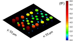
LNE with the support of METAS proposes a Good Practice Guide (GPG) to carry out Scanning Microwave Microscopy (SMM) based capacitance measurements with a demonstrated traceability to the international system of units (SI), a prerequisite for ensuring the comparability of results for measurements carried out in different places and at different points in time. The two National Metrology Institutes currently develop nanoscale impedance metrology using two types of SMM, cantilever based SMM (LNE) and tuning-fork based SMM (METAS).
The GPG can be downloaded from the ADVENT website: http://projects.lne.eu/jrp-advent/tools-publications/. In this guide, a general description of the experimental set-up is given, the calibration method developed for nanoscale capacitance measurements based on SMM detailed, and the calibration results on micrometer sized capacitors together with the main contributions to the uncertainty budgets are presented.
Submitted by François Piquemal, Laboratoire National de Métrologie et d’Essais (LNE), France
